Table of Contents
- 1.0 EPM1270F256C4N Datasheet & Core Features
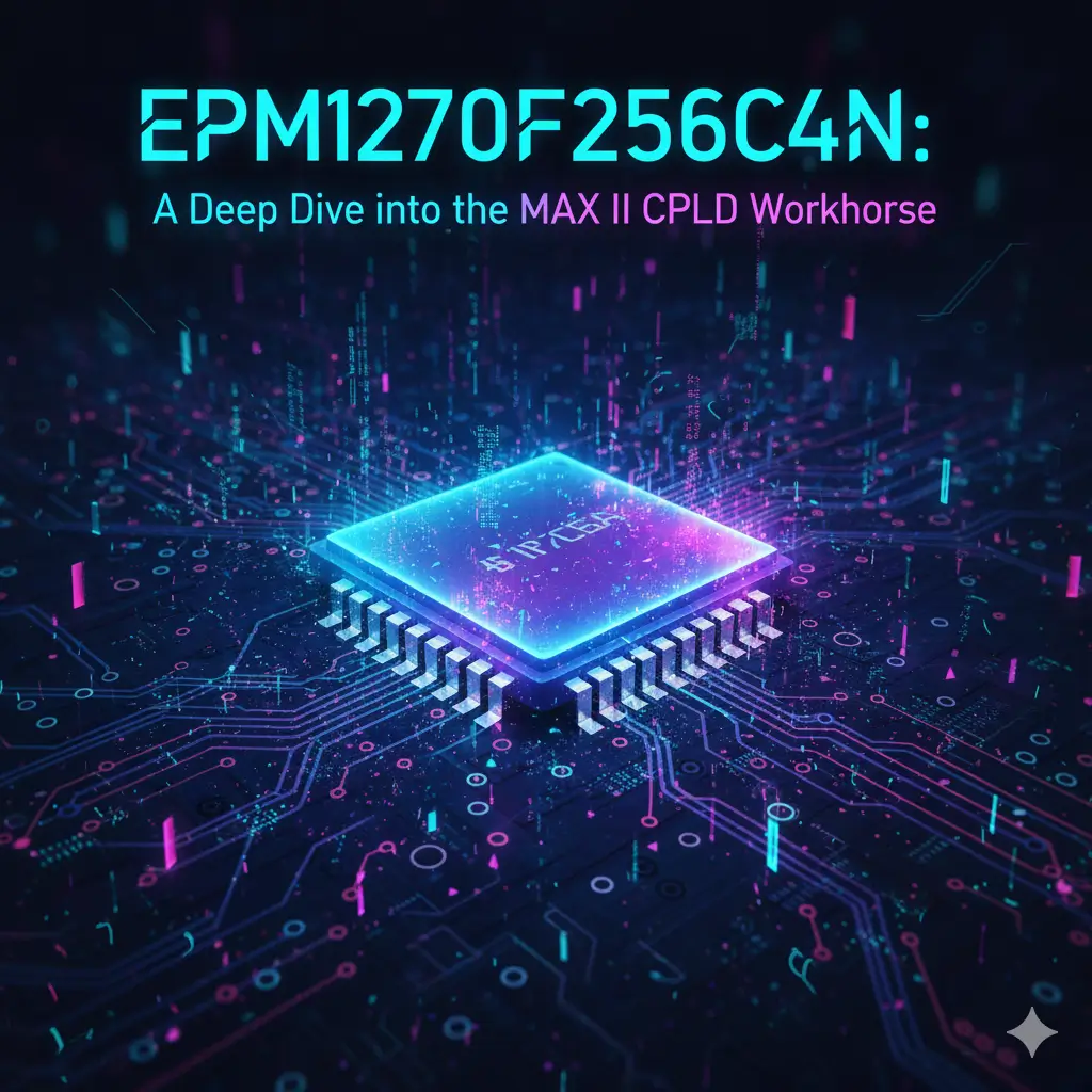
- 1.1 What is the EPM1270F256C4N?
- 1.2 The Altera MAX II CPLD Family Explained
- 1.3 Key Specifications (LEs, Memory, Voltage)
- 2.0 Why Choose the MAX II? (Non-Volatile, Instant-On)
- 2.1 The Non-Volatile Advantage (Flash Core)
- 2.2 EPM1270F256C4N vs. MAX V: A Comparison
- 2.3 Common Applications
- 3.0 EPM1270F256C4N Pinout (FBGA-256 Package)
- 3.1 256-Ball FBGA Pin Diagram
- 3.2 Key Pin Functions: Power, JTAG, and I/O
- 4.0 EPM1270F256C4N Programming and Software
- 4.1 Required Software: Altera Quartus II
- 4.2 JTAG Configuration and Programming
- 4.3 Finding a Replacement or Equivalent
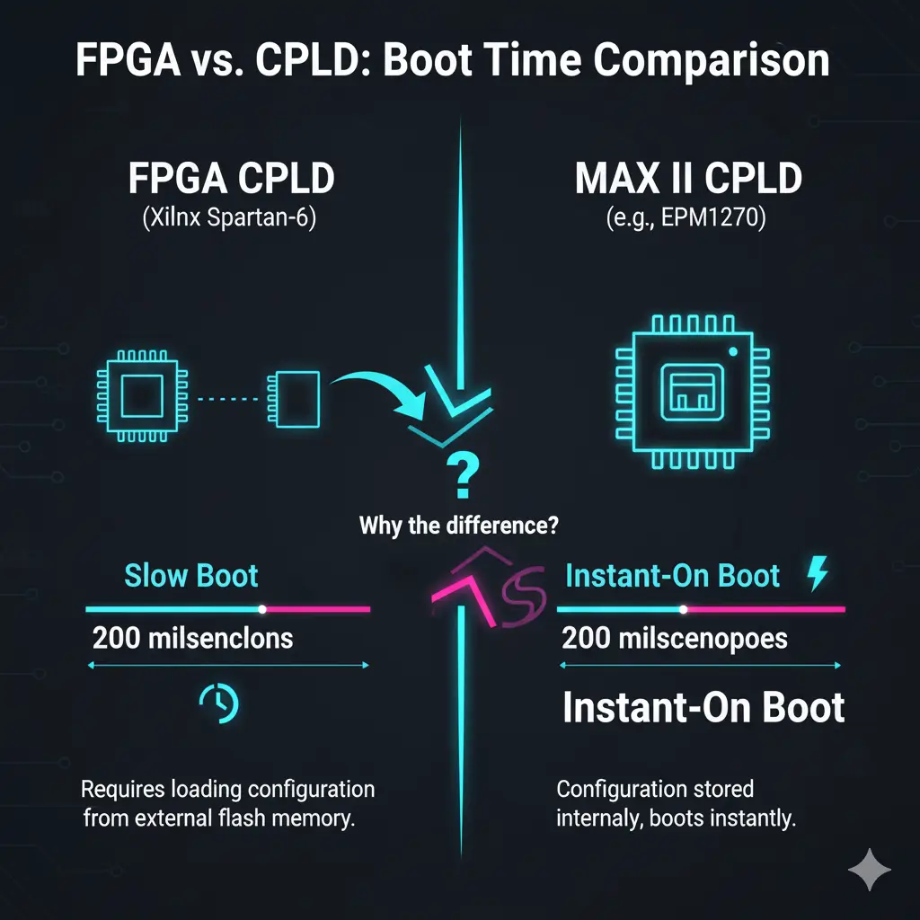
When you're designing an embedded system, your choice of logic device is critical. You might be tempted by the massive density of a modern FPGA, but what about boot-up time? What about power-on sequencing and system control? Many FPGAs are SRAM-based, meaning they are "blank" at power-on and must load their configuration from an external flash chip, a process that can take hundreds of milliseconds. For a system that needs to be "instant-on," this is a non-starter.
This is the exact problem that the EPM1270F256C4N MAX II CPLD was built to solve. As a CPLD (Complex Programmable Logic Device), it's a member of a different class of programmable logic. The global CPLD market, while mature, remains a vital part of the embedded systems landscape, especially for control and "glue logic" applications. In fact, by 2023, the need for fast, reliable, low-cost logic in IoT and industrial control has kept these devices in high demand.
The EPM1270F256C4N is a workhorse from this family, offering a powerful combination of logic, memory, and instant-on capability. This guide is your technical deep-dive into its datasheet, specs, and pinout, explaining why this CPLD is still a go-to choice for engineers today.
1.0 EPM1270F256C4N Datasheet & Core Features
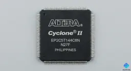
The EPM1270F256C4N is a high-density, low-cost CPLD from the Altera MAX II family (Altera is now part of Intel). Unlike FPGAs, which are like a blank canvas, CPLDs are more like a structured set of logic blocks, making them highly deterministic and fast for control-path applications.
1.1 What is the EPM1270F256C4N?
At its core, the EPM1270F256C4N is a non-volatile, instant-on CPLD. This is its single most important feature.
- Non-Volatile: It stores its configuration in on-chip flash memory. It does not need an external boot PROM or flash chip.
- Instant-On: Because the configuration is on-chip, it's ready to operate almost instantly at power-up (in microseconds).
- 1270 Logic Elements: It provides 1,270 Logic Elements (LEs), which is a significant amount of logic for tasks like I/O expansion, state machines, and power sequencing.
- F256 Package: It comes in a 256-pin FineLine BGA package, offering a high I/O count in a small footprint.
1.2 The Altera MAX II CPLD Family Explained
The MAX II family was designed to bridge the gap between traditional CPLDs and low-density FPGAs. It combines the best of both worlds:
- Non-volatile, instant-on architecture (like a CPLD).
- Higher logic density and on-chip RAM (like an FPGA).
- Low power consumption, making it ideal for battery-powered or thermally constrained designs.
This combination makes it perfect for "housekeeping" tasks in a larger system, such as managing the power-on sequence for a big, power-hungry FPGA or processor.
1.3 Key Specifications (LEs, Memory, Voltage)
When you're looking at the EPM1270F256C4N datasheet, these are the specs that matter.
| Parameter | Specification |
|---|---|
| Family | MAX II |
| Logic Elements (LEs) | 1,270 |
| Macrocells (Equivalent) | 980 |
| Total RAM Bits | 8,192 (8 kbits) |
| Max User I/O Pins | 212 |
| Core Voltage (VCCINT) | 1.8V |
| I/O Voltage (VCCIO) | 1.5V, 1.8V, 2.5V, or 3.3V |
| Speed Grade | -4 (Fast) |
| Package | 256-pin FineLine BGA (FBGA) |
| Temperature | Commercial (0°C to 85°C) |
2.0 Why Choose the MAX II? (Non-Volatile, Instant-On)
As an engineer, I've run into this exact problem: my main processor needs 10 different "power good" signals from 10 different power supplies before it can boot. A standard FPGA can't do this, because it isn't even booted itself! This is the job for a MAX II.
2.1 The Non-Volatile Advantage (Flash Core)
Let's use an analogy. An SRAM-based FPGA is like a brilliant professor who has amnesia every morning. You have to hand them their "configuration" (their notes) from an external flash drive every single time they wake up. This takes time.
A MAX II CPLD (like the EPM1270F256C4N) is a seasoned veteran who wakes up and already knows their job. The configuration is stored internally. This is the "instant-on" capability that makes it perfect for:
- Power-Up Sequencing: Controlling the order in which power supplies are turned on.
- System Control: Monitoring "power good" signals, handling reset logic, and managing system clocks.
- "Glue Logic": Connecting a CPU to peripherals that use different logic standards.
- I/O Expansion: Taking a serial I²C or SPI bus and expanding it to 32 parallel I/O lines.
2.2 EPM1270F256C4N vs. MAX V: A Comparison
The MAX V is the successor to the MAX II. If you're starting a new design, you might choose the MAX V. But the EPM1270 is a proven, reliable part often used for maintenance or as a pin-compatible drop-in for other MAX II devices.
| Feature | EPM1270F256C4N (MAX II) | MAX V (5M1270ZF256) |
|---|---|---|
| Architecture | 1.8V Flash Core | 1.8V Flash Core |
| Logic Elements (LEs) | 1,270 | 1,270 |
| User Flash Memory | 8 kbits | 56 kbits |
| Internal Oscillator | No | Yes (Integrated) |
| I/O Banks | 8 | 2 |
| Status | Mature / Legacy | In Production |
The takeaway: They have the same logic capacity (1270 LEs) and are often pin-compatible, but the MAX V integrates an oscillator and has more user flash, making it a good migration path if you're forced to redesign.
2.3 Common Applications
- System & Power Management: The #1 use case.
- Interface Bridging: Connecting 3.3V logic to 1.8V logic.
- Bus Control: Managing I²C, SPI, or simple parallel buses.
- I/O Expansion for microcontrollers.
- Simple State Machines and protocol logic.
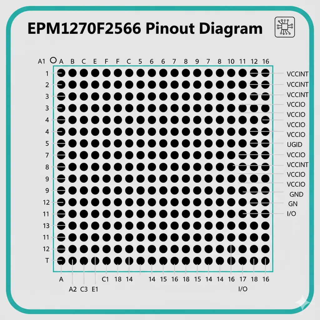
3.0 EPM1270F256C4N Pinout (FBGA-256 Package)
The EPM1270F256C4N pinout is for a 256-ball FineLine BGA (FBGA) package. This is a high-density, 1.0mm pitch package. When you're debugging, you'll be probing vias, not the pins themselves.
3.1 256-Ball FBGA Pin Diagram
3.2 Key Pin Functions: Power, JTAG, and I/O
When troubleshooting a board with this CPLD, these are the pins you check first.
| Pin Type | Name(s) | Function |
|---|---|---|
| Core Power | VCCINT | 1.8V core logic supply. Must be stable. |
| I/O Power | VCCIO (Banks 1-8) | 1.5V to 3.3V. Each of the 8 I/O banks can have a different voltage. |
| Ground | GND | Numerous ground pins. All must be connected. |
| JTAG | TCK, TDI, TDO, TMS | The JTAG programming/test port. This is how you load your design. |
| I/O | IO_... | User I/O pins. There are up to 212 available. |
Expert Tip: The VCCIO banks are the key to the MAX II's flexibility. You can have Bank 1 powered at 3.3V to talk to an old microcontroller, while Bank 2 is powered at 1.8V to talk to a new sensor, all on the same chip.
4.0 EPM1270F256C4N Programming and Software
This is the most critical part for any engineer working with this device, whether for a new design or for maintenance.
4.1 Required Software: Altera Quartus II
You must use the Altera (Intel) Quartus II software.
- Software Name: Altera Quartus II or Intel Quartus Prime (Lite).
- Compatible Version: The MAX II family is a mature device. It is fully supported by the free Quartus II v13.0sp1, which is a stable, well-known environment. It is also supported by the latest Intel Quartus Prime Lite editions.
- Hardware: You need a compatible JTAG programming cable, such as the Altera USB-Blaster or a Terasic USB-Blaster.
4.2 JTAG Configuration and Programming
Here is the basic "How-To" for programming the chip on your board:
- Install Software: Download and install the Intel Quartus Prime Lite software.
- Create Project: Start a new project and select the
EPM1270F256C4Nfrom the device list. - Write Code: Write your logic in VHDL or Verilog (or use the schematic editor).
- Compile & Assign Pins: Compile the design. Use the Pin Planner tool to assign your signals (e.g.,
LED_OUT,RESET_IN) to the physical package pins. - Program: Connect your USB-Blaster to the board's JTAG header. Open the Programmer tool in Quartus, detect your chip, and load the generated
.pof(Programmer Object File). Since it's non-volatile, the chip is now programmed permanently (until you reprogram it).
4.3 Finding a Replacement or Equivalent
As this is a mature part, you have two options if you can't find one.
- Direct Replacement: Source a genuine, identical EPM1270F256C4N. This is the best option for MRO as it requires no board changes.
- Pin-Compatible Upgrade: The 5M1270ZF256C4N (a MAX V device) is pin-compatible with the EPM1270F256C4N. You can often use it as a replacement, but you must recompile your design in Quartus II, targeting the MAX V device.
Conclusion: The "Instant-On" Logic Workhorse
The EPM1270F256C4N CPLD is a powerful and reliable component that serves a critical function in the world of embedded systems. Its instant-on, non-volatile nature makes it the perfect "system manager" to handle the critical power-up and control tasks that SRAM-based FPGAs simply can't.
While it may be a mature device, its utility in new designs (for glue logic) and its critical role in MRO (for system repair) keep it in high demand. If you are designing a system that needs to be fast, reliable, and "instant-on," or if you are maintaining equipment that uses one, the MAX II is a proven solution.
If you are looking for this part or other reliable CPLDs, AichipLink has you covered. Explore our full catalog of CPLDs or contact us today for a quote on the genuine Altera components you need.

Written by Jack Elliott from AIChipLink.
AIChipLink, one of the fastest-growing global independent electronic components distributors in the world, offers millions of products from thousands of manufacturers, and many of our in-stock parts is available to ship same day.
We mainly source and distribute integrated circuit (IC) products of brands such as Broadcom, Microchip, Texas Instruments, Infineon, NXP, Analog Devices, Qualcomm, Intel, etc., which are widely used in communication & network, telecom, industrial control, new energy and automotive electronics.
Empowered by AI, Linked to the Future. Get started on AIChipLink.com and submit your RFQ online today!
Frequently Asked Questions
What is the EPM1270F256C4N?
The EPM1270F256C4N is a **non-volatile CPLD** (Complex Programmable Logic Device) from the Altera (now Intel) MAX II family. It features 1,270 Logic Elements (LEs), 8 kbits of user flash, and 212 I/O pins in a 256-pin FBGA package. Its C4 designation means Commercial temperature and a fast -4 speed grade.
What is the main advantage of the EPM1270F256C4N MAX II CPLD?
Its main advantage is its **non-volatile, instant-on architecture**. Unlike an FPGA, it does not need an external boot PROM. It stores its configuration in on-chip flash memory, making it ideal for system control, "glue logic," and power-up sequencing.
What software is used to program the EPM1270F256C4N?
The EPM1270F256C4N is programmed using the **Altera Quartus II** software or the modern **Intel Quartus Prime (Lite Edition)**. A common, stable version used for this family is Quartus II v13.0sp1.
What is the difference between EPM1270F256C4N and EPM1270F256C5N?
The only difference is the **speed grade**. The **C4** part is a faster speed grade than the **C5** part. A C4 part can always be used as a direct replacement for a C5 part, but you cannot replace a C4 with a C5, as it may be too slow for the circuit.
What is a replacement for the EPM1270F256C4N?
For MRO, the best replacement is an identical **EPM1270F256C4N**. A pin-compatible *upgrade* is the **5M1270ZF256C4N** from the MAX V family, but this requires you to recompile your original design file for the new chip.