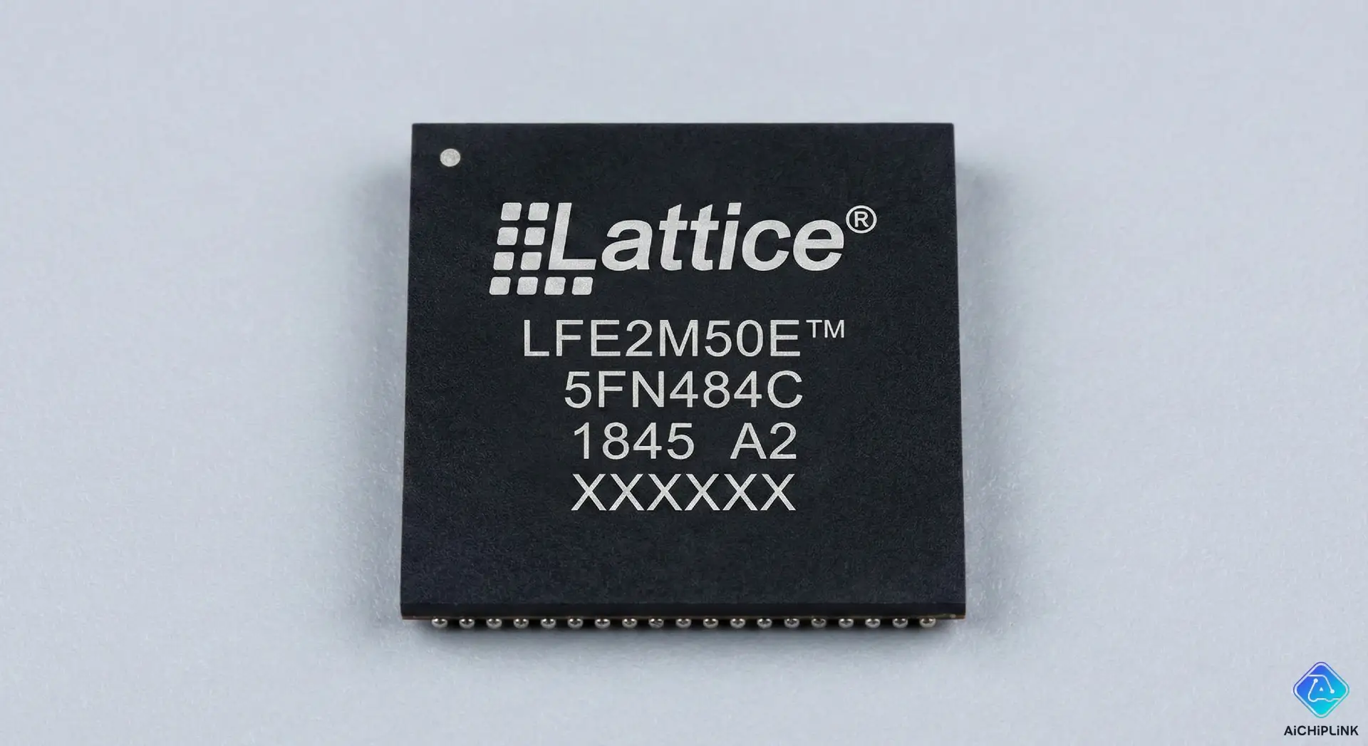
LFE2M50E-5FN484C FPGA Guide: Datasheet, SERDES Specs, and Pinout
The Lattice Semiconductor ECP2M family changed the FPGA landscape by integrating high-speed SERDES (Serializer/Deserializer) blocks into a low-cost, low-power FPGA fabric. At the heart of this family lies the LFE2M50E-5FN484C, a robust device offering 50,000 Logic Elements and advanced connectivity options.
Designed for applications ranging from wireless infrastructure to industrial video processing, the LFE2M50E-5FN484C remains a popular choice for designs requiring high-bandwidth I/O without the premium price tag of high-end FPGAs. This guide covers the essential specifications, pinout considerations, and programming tools for this component.
Table of Contents
- LFE2M50E-5FN484C Datasheet & Technical Specifications
- FPBGA484 Pinout & PCB Layout
- High-Speed SERDES Configuration
- Development Environment & Programming
- Conclusion
LFE2M50E-5FN484C Datasheet & Technical Specifications
The part number LFE2M50E-5FN484C indicates a specific configuration within the ECP2M family:
- LFE2M: Lattice ECP2M Family (Economy + Memory + SERDES).
- 50: ~50K Logic Elements (LUTs).
- E: Standard FPGA (SRAM based).
- -5: Speed Grade (Mid-range speed).
- F: FPBGA (Fine Pitch Ball Grid Array).
- N: Lead-Free (RoHS Compliant).
- 484: 484 Pins/Balls.
- C: Commercial Temperature (0°C to 85°C).
Key Specifications Table
| Feature | Specification |
|---|---|
| Logic Elements (LUTs) | 48,000 |
| Embedded Memory (EBR) | 2,211 Kbits |
| Distributed RAM | 63 Kbits |
| SERDES Channels | 8 Channels (up to 3.125 Gbps) |
| DSP Blocks | 168 (18x18 Multipliers) |
| User I/O | 270 |
| Core Voltage ($V_{CC}$) | 1.2V |
| Package | 484-ball FPBGA (23x23 mm) |
Price Analysis & Market Availability
The ECP2M series is known for its cost-effectiveness per SERDES channel. While it is a mature product, it is still widely active in the supply chain.
Note: Due to its popularity in legacy telecom equipment, stock levels can fluctuate. [Check Stock for LFE2M50E-5FN484C at Aichiplink] to view real-time inventory from authorized distributors.
ECP2M vs. ECP3: Migration Path
Engineers often compare ECP2M with the newer ECP3 family.
- ECP2M: Best for legacy designs requiring 5V tolerance on specific banks (via external resistors) and proven SERDES IP.
- ECP3: Offers lower power consumption and higher speed SERDES (3.2 Gbps+), but requires a PCB redesign due to pinout differences.
FPBGA484 Pinout & PCB Layout
The 484-ball FPBGA package uses a 1.0mm pitch, which is manageable for standard multi-layer PCB manufacturing.
FPBGA484 Footprint & Land Pattern
- Ball Grid: 22x22 array.
- PCB Layers: A minimum of 4-6 layers is recommended to effectively route the 270 User I/Os and manage the split power planes needed for the core, I/O, and SERDES.
Power Supply Decoupling
The ECP2M requires careful power management, especially for the analog SERDES blocks.
- $V_{CC}$ (Core): 1.2V. Requires bulk and ceramic capacitors close to the center balls.
- $V_{CCIO}$: Variable (3.3V, 2.5V, 1.8V, etc.) per bank.
- $V_{CCA}$ (Analog SERDES): Requires a clean, filtered 1.2V or 1.5V supply to minimize jitter.
High-Speed SERDES Configuration
The "M" in LFE2M stands for the integrated SERDES capability, which is the defining feature of this chip.
SERDES Capabilities
The LFE2M50E includes Quads of SERDES channels capable of running up to 3.125 Gbps. This allows the chip to support high-bandwidth protocols without external PHY chips.
Implementing PCIe & GbE
- PCI Express: The chip contains hard IP blocks to implement the Physical Coding Sublayer (PCS) for PCIe x1 or x4.
- Gigabit Ethernet: Supports SGMII interfaces directly, saving board space and BOM cost.
- Design Tip: Use the IPexpress tool within Lattice Diamond to generate the SERDES wrapper code automatically.
Development Environment & Programming
Unlike newer Lattice FPGAs (like Nexus) that use Radiant, the ECP2M family is supported by the mature Lattice Diamond software.
Lattice Diamond Setup
To program the LFE2M50E-5FN484C:
- Download Lattice Diamond Design Software (Standard license usually suffices for ECP2M).
- Use the HW-USBN-2B (USB programming cable).
- Generate the Bitstream (
.bit) and use the "Programmer" tool to flash the configuration to an external SPI Flash or directly to the FPGA SRAM.
Conclusion
The Lattice LFE2M50E-5FN484C represents a sweet spot in the FPGA market, offering significant logic density and integrated SERDES at a competitive price point. For engineers maintaining telecommunications gear or designing high-speed data acquisition systems, this chip remains a reliable workhorse.
Need to secure stock for your production run? Sourcing ECP2M components can be challenging as the series matures. Visit Aichiplink.com to browse our inventory of LFE2M50E-5FN484C and compatible Lattice components.

Written by Jack Elliott from AIChipLink.
AIChipLink, one of the fastest-growing global independent electronic components distributors in the world, offers millions of products from thousands of manufacturers, and many of our in-stock parts is available to ship same day.
We mainly source and distribute integrated circuit (IC) products of brands such as Broadcom, Microchip, Texas Instruments, Infineon, NXP, Analog Devices, Qualcomm, Intel, etc., which are widely used in communication & network, telecom, industrial control, new energy and automotive electronics.
Empowered by AI, Linked to the Future. Get started on AIChipLink.com and submit your RFQ online today!
Frequently Asked Questions
Is the LFE2M50E-5FN484C RoHS compliant?
Yes, the "N" in the part number suffix (5F**N**484C) indicates it is a Lead-Free, RoHS-compliant package.
Can I use Lattice ispLEVER software?
While ispLEVER Classic supported ECP2M, it is deprecated. It is highly recommended to use **Lattice Diamond** for all new designs and maintenance, as it provides better timing analysis and Place & Route algorithms.
What is the maximum SERDES speed of this device?
The -5 speed grade typically supports SERDES rates up to **3.125 Gbps**. If you need strictly 3.125 Gbps with higher margin, checking the datasheet for the -6 or -7 speed grades is advisable, though -5 is sufficient for standard 2.5 Gbps PCIe Gen1.
Does it have internal Flash memory?
No, the ECP2M is an SRAM-based FPGA. It requires an external boot device (SPI Flash or Parallel Flash) to load its configuration upon power-up.
What are the voltage requirements for the I/O banks?
The I/O banks are flexible and can be powered from 1.2V to 3.3V ($V_{CCIO}$). This allows the FPGA to interface with various logic standards like LVCMOS, LVTTL, SSTL, and HSTL.