You need to be very careful when you work with wide bandgap power devices. These devices have special problems like fast switching and high frequencies. Good equipment and correct calibration steps help you make fewer mistakes. People often make mistakes with floating differential measurements and common mode error. Here are some examples:
| Measurement Error | Cause |
|---|---|
| Difficulty in floating differential measurements | High common mode voltages and not enough common mode rejection at high bandwidth. |
| Dominance of common mode error | High frequency switching (fast turn ons and turn offs) can make measurements less accurate. |
You should watch out for defect dynamics when you test wide-bandgap devices. Defects can change how the device works, especially in tough situations. Careful testing and controlling the environment help lower these problems.
Key Takeaways
-
Use high-speed probes to get correct measurements. They help you see fast signals in wide bandgap devices.
-
Calibrate your testing setup to lower mistakes. Good calibration gives you data you can trust and cuts down on unwanted effects.
-
Control the testing area. Keep the temperature steady so you do not get wrong results in device performance.
-
Use good shielding and grounding methods. This stops noise and interference from changing your test results.
-
Get devices ready before you test them. Clean and handle them well to get correct results and stop damage.
Measurement Challenges in Wide Bandgap Power Devices
Fast Switching and High Bandwidth
When you use wide bandgap power devices, you face special problems. Devices like SiC and GaN switch much faster than silicon ones. Fast switching can make voltage and current probes out of sync. This can cause mistakes when you measure power and energy. You need good measurements to see how well the device works. OFF-state breakdown voltage tests show the highest voltage the device can take. This test is needed to make sure the device is safe for high-power jobs.
Parasitic Effects and Signal Integrity
Parasitic effects can make your measurements less trustworthy. High frequencies in these devices can bring in unwanted signals. You have to keep your signals clean. Parasitic inductance and capacitance can change your results. SiC and GaN devices have their own problems:
| Challenge Type | SiC Challenges | GaN Challenges |
|---|---|---|
| Reliability Issues | More heat stress because of Young’s modulus | Charge-trapping can change how well it works |
| Thermal Management | Good at moving heat but package can break | High power makes it hard to keep cool |
| Performance Characteristics | Works well at high heat | On-state resistance can get worse over time |
You should put your probes in the right place and use shields to help.
Thermal Metrology Issues
Heat and reliability are very important in wide bandgap testing. You must check thermal resistance and handle heat well. Normal ways to measure heat often do not work. Wide-bandgap materials move heat fast and have high contact resistance. You need special ways to measure heat right. High heat limits mean you may need to change your power modules. Good cooling keeps the device safe and stops it from breaking. How you handle heat affects how well and how long the device works.
| Measurement Challenge | Description |
|---|---|
| Thermal Resistance Measurement | Old ways do not work well because these materials move heat fast and have high contact resistance. |
| Anisotropic Thermal Conductivity | Heat moves differently in different directions, making it hard to measure. |
| Dominance of Contact Resistances | In thin films, contact resistance can be bigger than the real thermal resistance. |
| Need for Specialized Techniques | You need special ways to measure because normal ways do not work for these materials. |
Tip: Always check your cooling and setup before you test wide-bandgap devices.
Essential Equipment and Setup for Wide-Bandgap Testing
Probe Selection and Double-Pulse Testing
Picking the right probes is very important. High-speed probes help you see fast signals. Double-pulse testing shows how the device switches. It also shows how much energy it loses. A device power tester checks switching losses. An oscilloscope records what happens. An arbitrary function generator sends pulses to the gate. You need an inductor to act like a real circuit. Here is a table that lists the main equipment and what each one does:
| Equipment Type | Key Specifications |
|---|---|
| Device Power Tester (DPT) | Measures switching losses, checks energy lost when turning on, off, and during reverse recovery. |
| Inductor (L) | Acts like the circuit in the converter design. |
| Power Supply | Gives voltage for testing. |
| Arbitrary Function Generator | Sends pulses to the device gates. |
| Oscilloscope | Records and measures what happens. |
| WBG DPT Testing Software | Follows IEC 60747-9 rules and makes testing faster. |
| Parameter Analyzer | Tests materials, like resistivity and Hall mobility. |
| Keithley 4200A-SCS | Has tools for Van der Pauw resistivity and Hall Effect tests. |
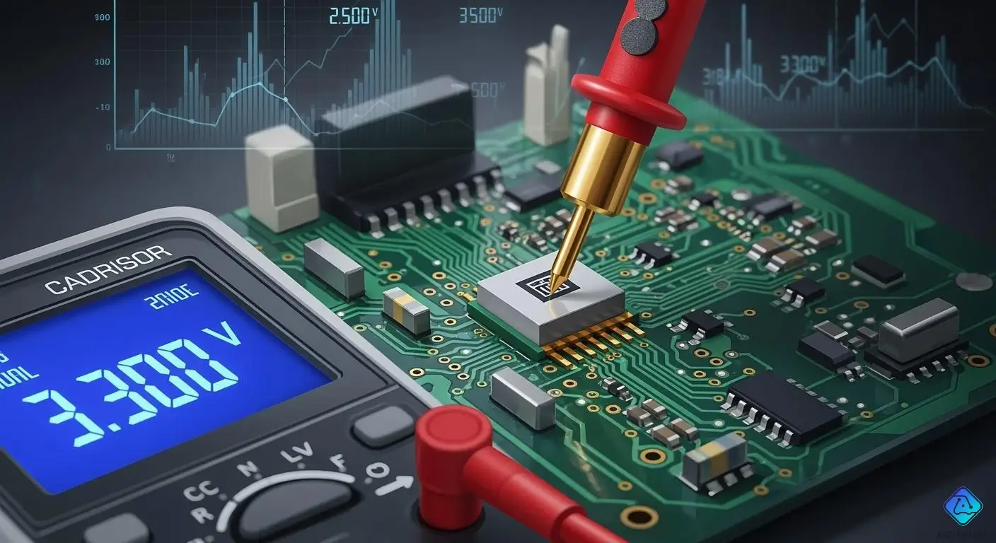
Tip: Always pick probes with high bandwidth and low capacitance for the best results.
Test Fixture Design and Calibration on FR4 PCB
A good test fixture helps you get correct data. FR4 PCB is often used for wide-bandgap testing. You must calibrate your fixture to fix errors from parasitic effects. Engineers use S-parameters to check packaged power devices. For GaN transistors, special calibration helps find parasitics. Here is a table that shows what you need to focus on during calibration:
| Evidence Description | Key Focus |
|---|---|
| Checking packaged power devices with S-parameters | Calibrate using special test fixtures on FR4 PCB for wide bandgap devices |
| Checking GaN packaged power transistors with S-parameters | Use calibration on FR4 PCB to find parasitics |
Note: A good layout for your test fixture helps lower parasitics and makes your results repeatable.
Shielding and Grounding for Reliable Data
Shielding your setup blocks outside signals. Good grounding keeps noise out of your measurements. Put your probes close to the device and use short wires. Shielding and grounding help keep your data clean. Always check your connections before you start testing.
-
Put metal shields around parts that are sensitive.
-
Connect all grounds at one spot to stop loops.
-
Make wires short and straight.
🛡️ Good shielding and grounding keep your measurements safe from interference.
Characterization Steps for Power Semiconductor Devices
Device Preparation and Handling
Before you test, get your devices ready. Clean them and look for any damage. Wide bandgap power devices can break if you are not careful. Wear gloves so you do not get them dirty. Put the device on an anti-static mat to stop static electricity. Always read the datasheet to know the voltage and current limits. If you use high power, make sure the device can take it. Good preparation gives you better i-v characterization results and keeps your devices safe.
Tip: Keep your devices in a dry place so moisture does not hurt how they work.
Calibration and Environmental Controls
Calibration is very important before you test. You need to check your equipment first. Use reference standards to make sure voltage and current readings are right. Test your device in a room where you can control the temperature. Keep the temperature the same to stop errors in i-v characterization. Wide-bandgap devices can change if it is too hot or wet. Use a climate chamber if you need to test heat and reliability. Power cycling helps you see how the device works over time. You can use calibration routines to check current and voltage at different temperatures.
-
Look at all cables and connectors for damage.
-
Use shielded cables to keep out noise.
-
Write down the room temperature before every test.
Note: Calibration and controlling the environment help you get the same results each time you test.
Executing Dynamic and Electrical Testing
You need different tests to see how power semiconductor devices work. Start with i-v characterization to see how the device acts with voltage and current. Use a source meter to change the voltage and measure the current. This shows how current and voltage are related and helps you find the device’s limits. Double pulse testing is very important for wide-bandgap devices. This test lets you measure energy loss when the device switches. You can also see how the device handles fast voltage changes.
Here is a table that lists the good things about common dynamic and electrical testing methods:
| Advantage | Description |
|---|---|
| Measures Energy Loss | Double pulse testing shows how much energy is lost when wide bandgap MOSFETs turn on and off. |
| Evaluates Dynamic Behaviors | This test helps you see how the device switches and acts during fast changes. |
| Automated Measurements | Automated measurements make testing more accurate and save time. |
You should use i-v characterization at different voltages to see how the device works. Write down the current for each voltage step. This helps you understand how the device works and how well it performs. If you want to test heat and reliability, do power cycling tests. These tests show what happens to the device after many cycles of voltage and current. Always check your setup before you start any test.
-
Use short wires to keep out noise.
-
Put probes close to the device.
-
Write down all voltage and current data for each i-v characterization test.
🧪 Good testing steps help you get reliable data and make your device work better.
Avoiding Common Errors in Wide-Bandgap Measurements
Probe Placement and Signal Integrity
You must be careful where you put probes when testing wide bandgap power devices. If probes are not in the right place, you might see problems. These problems include signal loading, ringing, or weird shapes on your voltage readings. These problems make your measurements less correct. They can also hide how your device really works.
If you do not put probes right, you can get more signal loading, ringing, and odd shapes because of bad grounding. These problems change your signals and make your results wrong.
Always keep your probe ground wires short and straight. Long ground loops can make pulses ring.
If you notice ringing on your pulse, try making your ground wire shorter. Shorter ground wires have less inductance and can make ringing happen at higher frequencies.
Always check your probe spots before you do high power tests. Short ground wires help you get better voltage and current numbers. Good probe spots help you get better test results.
Data Interpretation Pitfalls
You might have trouble when you look at your test results. Some mistakes are missing gate drive problems, not seeing reverse conduction, or missing voltage spikes and electromagnetic interference. These mistakes can make you think your power devices work better than they do. You can stop these mistakes by using negative off-state voltage to keep the device off. Series gate resistance and snubbers help you control voltage changes. Careful design helps you get real voltage and current results, especially when you test heat, reliability, or do power cycling.
Reducing Noise and Interference
Noise and interference can mess up your test results. You need to know where interference comes from. Use high-frequency parameter extraction to guess electromagnetic interference. PCB ground impedance and common-mode choke impedance can change your voltage numbers. You should keep wires short and use shields to block bad signals. Try to keep near-field couplings low to get better test results. These steps help you get clean data and see how your device really works during electrical tests.
Advanced Tips for Accurate Wide-Bandgap Characterization
High Bandwidth Sensor Techniques
You can get better results by using special sensors. Wide bandgap devices need sensors that work with fast changes. Coaxial Shunt Resistor (CSR) and Split-Core Probe (SCP) are two ways to sense current in power semiconductor devices. CSR can measure signals up to 1 GHz. SCP only goes up to 100 MHz. CSR can catch quick voltage spikes and fast current changes. This makes your measurements more accurate, especially in high power tests. CSR lowers turn-on switching loss by 52.4% and turn-off switching loss by 19.8% when current is high. At low current, CSR finds 74.4% more Eon because it sees fast events that SCP misses.
-
Use CSR for fast voltage and current tests.
-
Pick sensors with high bandwidth for better results.
-
Test at both high and low current to see all device actions.
Minimizing Parasitic Inductance and Capacitance
Parasitic inductance and capacitance can change your voltage numbers. They can also affect your tests. Keep wires short and put probes close to the device. Use a small layout to lower parasitic effects. Shielding blocks unwanted signals during tests. When you build your test setup, look for extra inductance and capacitance. These steps help you get more correct voltage and current data. You can see how your devices really work and avoid mistakes.
Tip: Always check your setup before power cycling or high power tests to keep parasitics low.
Software Tools for Data Analysis
You need good software to study your test data. LTspice and UALT are popular for wide bandgap device tests. LTspice lets you run time-domain simulations. It has built-in libraries for SiC and GaN transistors. UALT helps you automate LTspice simulations and makes changing settings easy. You can decode results for MATLAB analysis and graphs. These tools help you look at voltage and current waveforms. They also help you learn more about how your device works.
| Software Tool | Features |
|---|---|
| LTspice | Time-domain simulation studies, built-in libraries for SiC and GaN transistors, fast computing, strong convergence for tricky waveforms, not as easy to use as some commercial tools |
| UALT | Automates LTspice simulations, makes repeating tests easy, lets you change settings during tests, decodes LTspice results for MATLAB graphs and study |
Note: Use software to compare voltage and current data from different tests.
You can get good measurements with wide bandgap power devices if you follow simple steps. Use the right tools, get your devices ready, and make sure your testing area is controlled. Try advanced ways like making your process better to get improved results. New studies show you can get high linearity and good efficiency by using things like piranha solution treatment and annealing. When your data is reliable and repeatable, you can see how your devices work.
| Parameter | Value | Notes |
|---|---|---|
| Output Third-Order Intercept Point (OIP3) | 28 dBm | High linearity in RF applications |
| Power Gain (G_a) | 20.5 dB | Efficient β-Ga2O3 RF power MOSFET |
| Maximum Output Power (P_out) | 4.6 W/mm | Achieved at V_DS = 30 V, f = 2 GHz |
| Power Added Efficiency (PAE) | 50.5% | Effective power conversion |
| Process Refinement Techniques | Piranha solution, annealing | Improves output power by reducing interface traps |
Keep learning new things and changing your ways. Good measurements help you get the best from your devices.

Written by Jack Elliott from AIChipLink.
AIChipLink, one of the fastest-growing global independent electronic components distributors in the world, offers millions of products from thousands of manufacturers, and many of our in-stock parts is available to ship same day.
We mainly source and distribute integrated circuit (IC) products of brands such as Broadcom, Microchip, Texas Instruments, Infineon, NXP, Analog Devices, Qualcomm, Intel, etc., which are widely used in communication & network, telecom, industrial control, new energy and automotive electronics.
Empowered by AI, Linked to the Future. Get started on AIChipLink.com and submit your RFQ online today!


.png&w=256&q=75)

