Table of Contents
- 1.0 EP2C5F256C6 Datasheet Overview: The Cyclone II Workhorse
- 1.1 What is the EP2C5F256C6?
- 1.2 Decoding the Part Number: EP2C5F256C6
- 1.3 Key Features of the Altera Cyclone II Family
- 2.0 EP2C5F256C6 Pinout (FBGA-256 Package)
- 2.1 256-Ball FineLine BGA Pin Diagram
- 2.2 Key Pin Functions: Power, JTAG, and Configuration
- 3.0 EP2C5F256C6 Key Technical Specifications
- 3.1 Core Logic, Memory, and PLL Specs
- 3.2 Operating Conditions and Package
- 3.3 Obsolescence & Replacement Status
- 4.0 How to Program the EP2C5F256C6 FPGA
- 4.1 Required Software: Legacy Altera Quartus II
- 4.2 Configuration Devices (EPCS, etc.)
- 4.3 Common Applications
- 5.0 Frequently Asked Questions (FAQ)
If you're an engineer or technician working on industrial, medical, or automotive equipment that's been in the field for a decade, the EP2C5F256C6 FPGA is a part number you've likely encountered. This chip is a workhorse from the Altera Cyclone II family, a series that defined low-cost, high-volume FPGA applications in the mid-2000s.
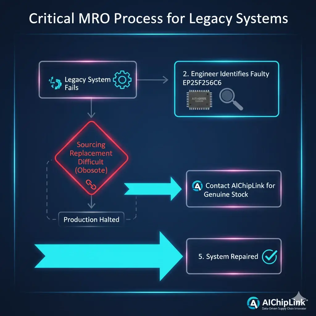
While it's not a chip you'd use in a brand-new design in 2025, the MRO (Maintenance, Repair, and Operations) market for these legacy systems is massive. The global industrial automation market, for example, relies on equipment with 10-20 year lifecycles. When a control board with an EP2C5F256C6 fails, you can't just "upgrade" it—you need a reliable, identical replacement to prevent costly downtime.
You're here for technical data, not a sales pitch. This guide is your engineering-focused deep-dive into the EP2C5F256C6 datasheet, covering its pinout, specifications, and the all-important legacy programming software you'll need to work with it.
1.0 EP2C5F256C6 Datasheet Overview: The Cyclone II Workhorse
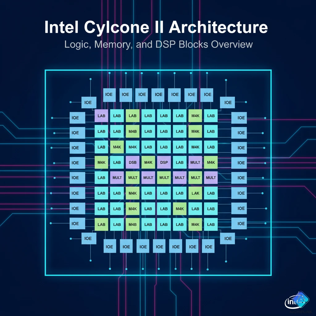
The EP2C5F256C6 is a legacy Field-Programmable Gate Array (FPGA) originally manufactured by Altera, which was later acquired by Intel. It is a member of the Cyclone II family, which was built on a 90-nm process and designed to be a low-cost solution for logic-intensive applications.
1.1 What is the EP2C5F256C6?
At its core, the EP2C5F256C6 is an SRAM-based FPGA. This means, like most FPGAs, its configuration is volatile and must be loaded from an external source at every power-on. It was designed to replace fixed-logic ASICs and CPLDs by offering a more flexible and reconfigurable solution at a mass-market price point.
Its key features were:
- Low Cost: The primary design goal of the Cyclone II series.
- Sufficient Density: Offered enough logic to implement complex state machines, protocol bridges, and data processing tasks.
- Embedded Memory: Included dedicated on-chip RAM blocks.
- PLLs: Integrated Phase-Locked Loops for flexible clock management.
1.2 Decoding the Part Number: EP2C5F256C6
The part number is a code that tells you exactly what the device is:
- EP2C: Identifies the device as an Altera Cyclone II.
- 5: Denotes the device density. In this case, it has 4,608 Logic Elements (LEs).
- F256: This is the package type: a 256-pin FineLine BGA (FBGA).
- C6: This is the speed grade and temperature range. "C" stands for Commercial (0°C to 85°C), and "-6" is the fastest speed grade for this device.
1.3 Key Features of the Altera Cyclone II Family
The Altera Cyclone II family was successful because it provided a well-balanced feature set for its price.
- Logic Elements (LEs): The fundamental building block, each containing a 4-input look-up table (LUT), a flip-flop, and carry-chain logic.
- M4K RAM Blocks: 4-kbit embedded memory blocks that can be configured as RAM, ROM, or FIFOs.
- Embedded Multipliers: Dedicated 18x18 multiplier blocks for efficient DSP (Digital Signal Processing).
- PLLs: On-chip PLLs for clock synthesis, deskewing, and frequency multiplication/division.
- Flexible I/O: Supports a wide range of I/O standards like LVDS, LVCMOS, and SSTL.
2.0 EP2C5F256C6 Pinout (FBGA-256 Package)
The EP2C5F256C6 pinout corresponds to the 256-ball FineLine BGA package. This is a surface-mount package where the pins are solder balls on the underside of the chip. Repairing or replacing these requires a BGA rework station and X-ray inspection.
2.1 256-Ball FineLine BGA Pin Diagram
The FBGA-256 is a 17x17 grid (with some balls missing). When you're probing a board, you'll be looking for vias that trace back to this footprint.
2.2 Key Pin Functions: Power, JTAG, and Configuration
When troubleshooting, you don't check all 172 I/O pins. You check the core support pins first.
| Pin Type | Name(s) | Function |
|---|---|---|
| Core Power | VCCINT | 1.2V core logic supply. This is the main power for the FPGA. |
| I/O Power | VCCIO (Banks 1-8) | 3.3V / 2.5V / 1.8V / 1.5V. Each I/O bank can be powered independently. |
| PLL Power | VCCA, VCCD | Dedicated analog and digital power for the PLLs. |
| Ground | GND | Numerous ground pins. All must be connected. |
| JTAG | TCK, TDI, TDO, TMS | The JTAG test/programming port. This is how you configure the chip. |
| Configuration | nCE, nCEO, MSEL0, MSEL1 | Pins that control how the FPGA loads its configuration from an external flash. |
| Config Data | DCLK, DATA0, nCS, ASDI | The pins used to feed the configuration data from a serial flash chip (like an EPCS). |
3.0 EP2C5F256C6 Key Technical Specifications
If you are sourcing a replacement, these are the EP2C5F256C6 specs you must match.
3.1 Core Logic, Memory, and PLL Specs
| Feature | Specification |
|---|---|
| Logic Elements (LEs) | 4,608 |
| Total RAM Bits | 119,808 (13 x M4K blocks) |
| Embedded Multipliers | 13 (18-bit x 18-bit) |
| PLLs | 2 |
| Maximum User I/O | 172 |
| Package | 256-pin FineLine BGA |
3.2 Operating Conditions and Package
- Core Voltage (VCCINT): 1.2V (±5%)
- I/O Voltage (VCCIO): 1.5V, 1.8V, 2.5V, or 3.3V
- Temperature Range: Commercial (0°C to 85°C)
- Speed Grade: -6 (Fastest)
3.3 Obsolescence & Replacement Status
Official Status: OBSOLETE / END-OF-LIFE (EOL)
The EP2C5F256C6 and the entire Cyclone II family are considered obsolete by Intel. They are Not Recommended for New Designs (NRND).
Why this matters to you: There is no new stock being manufactured. All parts available are from existing inventory. This makes finding a genuine, reliable part the single biggest challenge. For repair, you must source an identical EP2C5F256C6. A redesign to a modern chip (like a Cyclone 10 LP) would require a new PCB and a full software port.
4.0 How to Program the EP2C5F256C6 FPGA
This is the biggest hurdle for engineers new to legacy Altera parts. You cannot use modern Intel Quartus Prime software.
4.1 Required Software: Legacy Altera Quartus II
To program, compile, or even just test an EP2C5F256C6, you must use a specific legacy version of the Altera design software.
- Software Name: Altera Quartus II (not Intel Quartus Prime).
- Compatible Version: Version 13.0sp1 is the last version to support the Cyclone II family.
- OS Compatibility: This legacy software runs best on older operating systems like Windows 7. Running it in a virtual machine is a common solution.
- Programming Hardware: You need a compatible JTAG programming cable, such as the Altera USB-Blaster.
4.2 Configuration Devices (EPCS, etc.)
The EP2C5F256C6 is SRAM-based, so its configuration is volatile (lost on power-down). It needs to boot from an external non-volatile chip.
- Configuration Scheme: Typically uses Active Serial (AS) mode.
- Required Configuration Chip: It is designed to boot from an EPCS serial configuration device, such as the EPCS4SI8N.
- Boot Process: At power-on, the FPGA acts as the master, provides a clock, and pulls the configuration data from the EPCS chip into its own SRAM.
4.3 Common Applications
You will find this FPGA in a wide range of long-life equipment:
- Industrial Automation: PLCs, motor control units, and HMI displays.
- Video Processing: Simple video scalers, format converters, and test pattern generators.
- Medical Equipment: Patient monitors, diagnostic machines, and lab equipment.
- Automotive: (Though C6 is commercial grade, "I" grade automotive parts were common).
- "Glue Logic": The most common use—replacing dozens of small logic chips to connect a CPU to its peripherals, memory, and I/O.
Conclusion: A Critical Legacy Component
The EP2C5F256C6 FPGA is a true workhorse of the 2000s. Its role has shifted from a low-cost innovation to a critical MRO component for maintaining the world's industrial, medical, and communications infrastructure.
Understanding its legacy status, 1.2V core, and specific programming software is essential for any engineer or technician tasked with its maintenance. As these parts become scarcer, the risk of production line stoppages due to counterfeit or low-quality components increases.
You need a supply chain partner who understands the challenges of sourcing obsolete FPGAs. If your system is down and you need a reliable, genuine EP2C5F256C6, don't waste time with unverified brokers.
Explore our full catalog of FPGAs or contact AichipLink today for a quote on the genuine legacy components you need to keep your systems running.

Written by Jack Elliott from AIChipLink.
AIChipLink, one of the fastest-growing global independent electronic components distributors in the world, offers millions of products from thousands of manufacturers, and many of our in-stock parts is available to ship same day.
We mainly source and distribute integrated circuit (IC) products of brands such as Broadcom, Microchip, Texas Instruments, Infineon, NXP, Analog Devices, Qualcomm, Intel, etc., which are widely used in communication & network, telecom, industrial control, new energy and automotive electronics.
Empowered by AI, Linked to the Future. Get started on AIChipLink.com and submit your RFQ online today!
Frequently Asked Questions
What is the EP2C5F256C6?
The EP2C5F256C6 is a legacy FPGA from the **Altera (now Intel) Cyclone II** family. It features **4,608 Logic Elements (LEs)**, 119,808 bits of RAM, and 172 user I/O pins, all housed in a **256-pin FineLine BGA (FBGA)** package. It is a 1.2V core device with a "C6" (commercial, fast) speed grade.
Is the EP2C5F256C6 obsolete?
Yes, the **EP2C5F256C6** and the entire Cyclone II family are **obsolete (End-of-Life)**. They are no longer manufactured and are Not Recommended for New Designs (NRND). Their primary market is for the maintenance, repair, and replacement (MRO) of existing equipment.
What software do I use to program the EP2C5F256C6?
You must use a legacy version of the **Altera Quartus II** development software, such as **v13.0sp1**. Modern Intel Quartus Prime software does **not** support the Cyclone II family. You will also need a programming cable like the Altera USB-Blaster.
What is the difference between EP2C5F256C6 and EP2C5T144C8N?
Both are Cyclone II FPGAs with 4,608 LEs. The main differences are the package, pin count, and speed. * **EP2C5F256C6:** **256-pin BGA** package, 172 I/O, **-6 speed grade (fastest)**. * **EP2C5T144C8N:** **144-pin TQFP** package, 89 I/O, **-8 speed grade (slowest)**. They are not pin-compatible and are intended for different applications.
What is the configuration device for an EP2C5F256C6?
The EP2C5F256C6 is typically configured using an Altera **EPCS** (Serial Configuration) device, such as an **EPCS1** or **EPCS4**. The FPGA reads its configuration data from this external flash chip at every power-on.