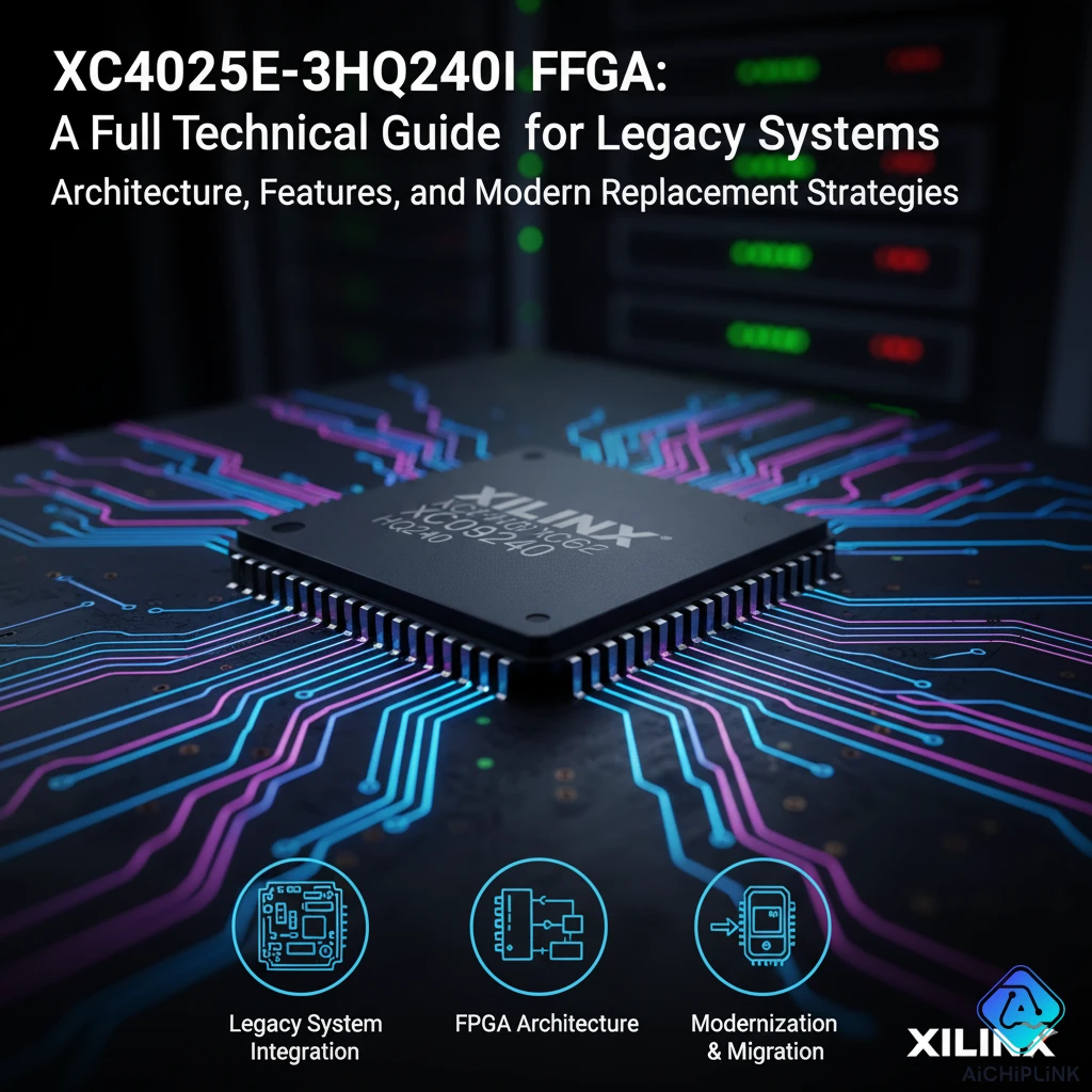
1.0 What is the XC4025E-3HQ240I? (Datasheet Explained)
Ever opened a 20-year-old piece of industrial machinery, a piece of telecom gear, or a piece of medical testing equipment and found a chip you've never seen in a modern design? Chances are, you might have run into the XC4025E-3HQ240I. This isn't a component you'll find in a new smartphone; it's a veteran, a legacy workhorse from the Xilinx XC4000E family of FPGAs.
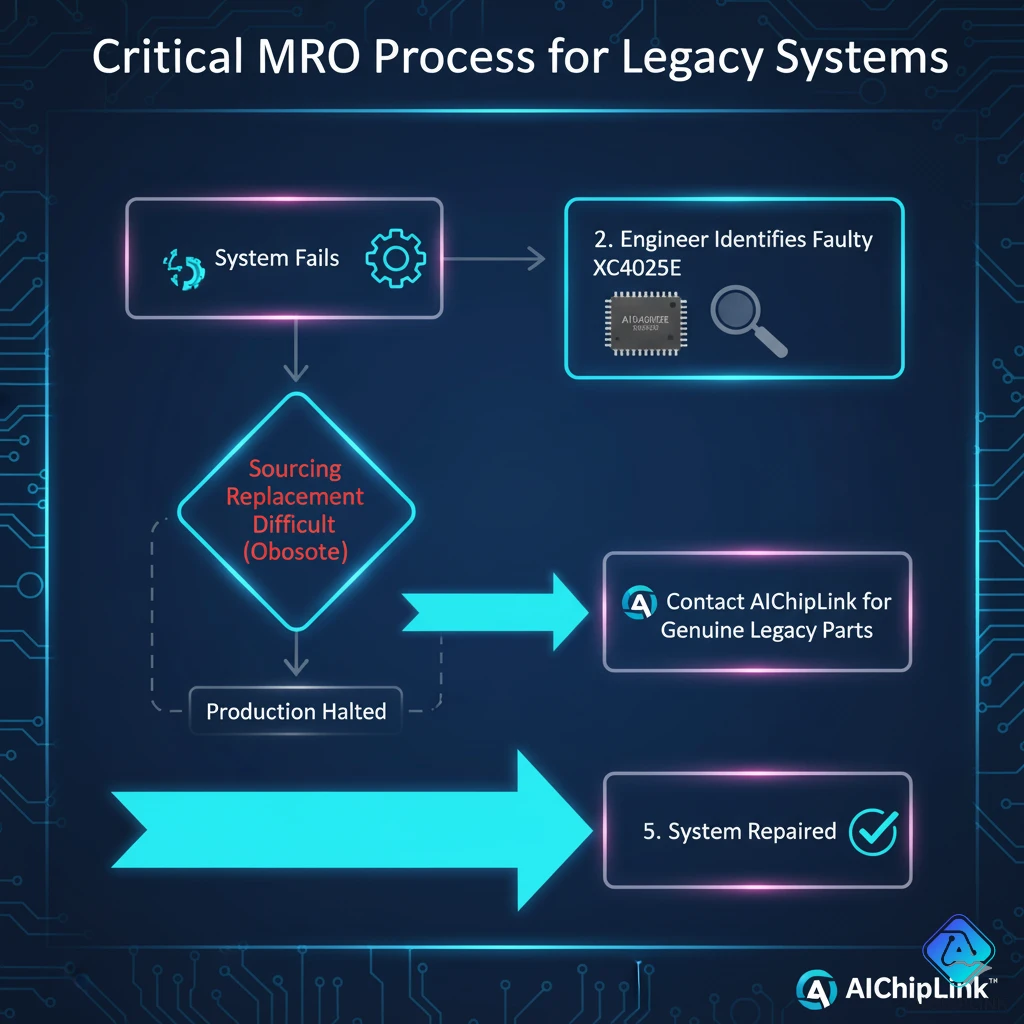
In 2025, the market for maintaining, repairing, and operating (MRO) this legacy equipment is a massive, multi-billion dollar industry. For an engineer, technician, or supply chain manager, a line-down situation can be disastrous. The problem is often a single failed component. That's why understanding this "obsolete" chip isn't just a history lesson—it's a critical business necessity.
This guide is your technical deep-dive into the XC4025E-3HQ240I and its datasheet. We will cover its specifications, pinout, and—most importantly—the legacy software and replacement strategies you need to know to keep your systems running.
1.1 The Xilinx XC4000E Family: A 5V Workhorse
The XC4000E series, which includes the XC4025E, was one of the most popular and dominant FPGA families of the mid-1990s. Its success was built on a few key features that were revolutionary at the time:
- 5V Operation: It was a true 5V device, operating on a 5V core (VCCINT) and with 5V I/O (VCCO). This made it perfect for interfacing with the ubiquitous 5V TTL and CMOS logic of that era.
- SRAM-Based: Like modern FPGAs, it's SRAM-based, meaning its configuration is volatile and must be loaded at power-up from an external source.
- CLB Architecture: It introduced the flexible Configurable Logic Block (CLB) architecture that Xilinx is famous for, which included function generators (Look-Up Tables), flip-flops, and fast-carry logic.
- On-Chip RAM: It featured both distributed RAM (using the CLBs) and dedicated BlockRAM, allowing for efficient on-chip data storage.
1.2 Decoding the Part Number: XC4025E-3HQ240I
The part number tells you everything you need to know:
- XC: Xilinx
- 4025E: The device family (XC4000E) and density (25,000 typical gates).
- -3: The speed grade (a standard, relatively fast grade for this family).
- HQ: The package type, a High-Heat 240-pin Quad Flat Pack (HQFP). This is a robust package designed for good thermal dissipation.
- 240: The pin count.
- I: The temperature grade, Industrial (-40°C to 85°C). This is why you find it in harsh factory environments.
1.3 Obsolescence Status in 2025: A Critical MRO Component
This is the most important fact you need to know: The XC4025E-3HQ240I and the entire XC4000E family are completely obsolete and End-of-Life (EOL). They are Not Recommended for New Designs (NRND).
Modern FPGAs are worlds apart, running on 1.2V or lower, with millions of logic cells. The value of the XC4025E-3HQ240I today is purely as a service part. Because it's no longer manufactured, finding a genuine, reliable replacement is a significant supply chain challenge. You must work with a trusted distributor who specializes in obsolete components.
2.0 XC4025E-3HQ240I Key Technical Specifications
When you are sourcing a replacement part, you must match the XC4025E specs exactly. Here is the critical information from the legacy datasheet.
2.1 Core Logic, Memory, and I/O Specs
This device was a powerhouse for its day, designed to consolidate dozens, if not hundreds, of smaller 74-series logic chips into one.
| Specification | Value |
|---|---|
| Family | XC4000E |
| Typical Logic Gates | 25,000 |
| Logic Cells | 2,432 |
| Configurable Logic Blocks (CLBs) | 1,024 (a 32x32 matrix) |
| Total Flip-Flops | 2,816 |
| Max On-Chip RAM | 65,536 bits (64 kbits) |
| Max User I/O | 193 |
| Technology | 0.5 µm SRAM-based CMOS |
2.2 Operating Voltage and Temperature
This is a critical, non-negotiable specification for a replacement part.
- Core Supply Voltage (VCCINT): 5.0V (nominal, ±5%)
- I/O Supply Voltage (VCCO): 5.0V (nominal, ±5%)
- Temperature Grade (I): Industrial (-40°C to 85°C)
This is not a 3.3V or 1.8V part. It is a true 5V device. Using a modern, low-voltage FPGA would require a complete board redesign with multiple voltage regulators and level shifters.
3.0 XC4025E-3HQ240I Pinout (HQ240 Package)
If you're troubleshooting a dead board, the XC4025E-3HQ240I pinout is your roadmap. The HQ240 package is a large, 240-pin quad flat pack.
3.1 HQ240 Package Pin Functions
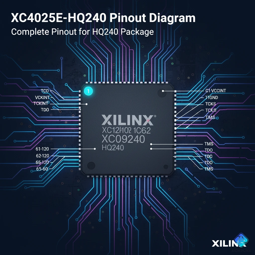
3.2 Key Pins: Power, JTAG, and Configuration
When a board fails, you don't probe all 193 I/O pins. You check the "housekeeping" pins first.
| Pin Type | Pin Name(s) | Function |
|---|---|---|
| Power | VCC, GND | There are multiple VCC (5V) and GND pins. All must be connected. |
| JTAG | TDI, TDO, TCK, TMS | The 4-pin JTAG port. Used for programming, debugging, and testing. |
| Mode | M0, M1, M2 | These pins are hard-wired on the PCB to set the configuration mode at boot-up. |
| Config | CCLK, DIN, DONE | CCLK (Configuration Clock) and DIN (Data In) are used to load the bitstream from a PROM. |
| Status | DONE | This pin goes high when the FPGA has successfully loaded its configuration. If this pin is low, the FPGA is not running. |
4.0 Programming and Replacement Guide
Here is the most critical information for an engineer in 2025. How do you program this chip, and what do you do if you can't find one?
4.1 How to Program the XC4025E-3HQ240I
Because this is an SRAM-based FPGA, its configuration is volatile (it's erased when power is lost). It must be programmed every time it's powered on.
- Obtain Legacy Software: You cannot use modern Xilinx Vivado. You must find and install the original Xilinx Foundation Series software or the later Xilinx ISE (Integrated Software Environment), typically a version from the early 2000s (like ISE 4, 5, or 6).
- Design & Compile: Create your design in VHDL or Verilog using the legacy software. Target the
XC4025E-3HQ240Idevice. - Generate Bitstream: Compile the design to generate a
.bit(for JTAG loading) or.mcs(for PROM programming) file. - Load Configuration: At power-up, the FPGA automatically loads its configuration from an external serial PROM (like a Xilinx XC17S00XL series chip) or can be programmed by a host microcontroller. For testing, you can load the
.bitfile directly using a Xilinx JTAG programmer.
4.2 Required Software: Xilinx Foundation or ISE
I must emphasize this: Modern tools will not work. The XC4025E-3HQ240I is a legacy device. You must find, install, and often run the old Xilinx ISE software on a legacy operating system (like Windows XP or Windows 7 32-bit) in a virtual machine. This is non-negotiable and the single biggest hurdle for working with these parts.
4.3 Finding a Replacement or Equivalent
You have one main challenge: this part is obsolete.
- Direct Replacement: The only 100% drop-in, pin-compatible replacement is another XC4025E-3HQ240I. You may be able to use a different speed grade (like a
-2or-4), but you must verify timing. - Modern Redesign: There is no modern, pin-compatible replacement. A redesign would mean using a modern, low-voltage FPGA (like an Artix-7 or Cyclone 10) and redesigning the entire PCB to accommodate the new footprint, voltage levels (1.2V, 3.3V), and configuration scheme. This is a massive engineering effort.
| Parameter | XC4025E-3HQ240I (Legacy) | Modern FPGA (e.g., Artix-7) |
|---|---|---|
| Core Voltage | 5.0V | ~1.0V |
| Logic Cells | 2,432 | 50,000+ |
| Block RAM | 64 kbits | 2,000 kbits+ |
| Software | Xilinx ISE (Legacy) | Xilinx Vivado (Modern) |
| Status | Obsolete | In Production |
5.0 Common Applications (Where to Find It)
You will find the XC4025E-3HQ240I and its XC4000E siblings in long-life industrial, medical, and telecom equipment built in the 90s and 2000s.
- Industrial Control: The brains of PLCs, CNC machines, and robotic arms.
- Telecommunications: In legacy switching hardware, base station controllers, and T1/E1 line cards.
- Test & Measurement: The logic core for older oscilloscopes, spectrum analyzers, and protocol testers.
- Aerospace & Defense: In long-service-life avionics and ground control systems.
Conclusion: The MRO Challenge of a 5V Workhorse
The XC4025E-3HQ240I FPGA is a true classic. It represents an era of 5V logic that was built to last—and it has. For engineers and technicians supporting these systems, the challenge isn't performance; it's availability. The skills required to program and troubleshoot these FPGAs are specialized, and sourcing genuine, reliable parts is the number one priority.
Don't let a single obsolete chip be the reason your critical infrastructure fails. If you are in the difficult position of needing to find a replacement for the XC4025E-3HQ240I or any other legacy component, you need a partner who understands the MRO market.
Contact AichipLink today. We are experts in sourcing hard-to-find and obsolete FPGAs, and we can help you get the genuine parts you need to keep your systems operational.

Written by Jack Elliott from AIChipLink.
AIChipLink, one of the fastest-growing global independent electronic components distributors in the world, offers millions of products from thousands of manufacturers, and many of our in-stock parts is available to ship same day.
We mainly source and distribute integrated circuit (IC) products of brands such as Broadcom, Microchip, Texas Instruments, Infineon, NXP, Analog Devices, Qualcomm, Intel, etc., which are widely used in communication & network, telecom, industrial control, new energy and automotive electronics.
Empowered by AI, Linked to the Future. Get started on AIChipLink.com and submit your RFQ online today!
Frequently Asked Questions
What is the XC4025E-3HQ240I?
The XC4025E-3HQ240I is a legacy 5V, SRAM-based **FPGA** from the Xilinx XC4000E family. It features 25,000 typical gates, 2,432 logic cells, and 193 user I/O pins. It is in a 240-pin High-Heat Quad Flat Pack (HQFP) and is rated for the industrial temperature range.
Is the XC4025E-3HQ240I obsolete?
Yes, this part is completely obsolete and End-of-Life (EOL). It is no longer manufactured by Xilinx/AMD and is not recommended for new designs. Its only use today is as a replacement part for maintenance and repair (MRO).
What software do I use to program the XC4025E-3HQ240I?
You must use the legacy Xilinx ISE (Integrated Software Environment) software, version 6 or older. The modern Xilinx Vivado suite does not support the XC4000E family. You may also need a 32-bit OS (like Windows XP/7) to run the old software.
Is the XC4025E-3HQ240I 5V tolerant?
The XC4025E-3HQ240I is a true 5V device. Its core (VCCINT) and I/O banks (VCCO) both operate at a nominal 5V, making it directly compatible with 5V TTL and CMOS logic systems.
What is a replacement for the XC4025E-3HQ240I?
There is no direct, pin-for-pin modern replacement. For a repair, you must source an identical XC4025E-3HQ240I. A full system redesign would be required to "upgrade" to a modern, low-voltage FPGA, which is a major engineering project.