Table of Contents
- 1.0 What is the XCV50-6TQ144C? (Datasheet Explained)
- 1.1 The Original Virtex Family: The 2.5V Pioneer
- 1.2 Decoding the Part Number: Speed Grade -6 & TQ144
- 1.3 Obsolescence Status: A Vital MRO Component
- 2.0 XCV50-6TQ144C Key Technical Specifications
- 2.1 Core Logic, Block RAM, and DLLs
- 2.2 Operating Voltage: The 2.5V Core Constraint
- 3.0 Pinout and Package Details (TQ144)
- 3.1 Understanding the 144-Pin TQFP Package
- 3.2 Key Pin Functions: VCCINT, VCCO, and Configuration
- 4.0 Programming and Maintenance Guide
- 4.1 Required Software: Legacy Xilinx ISE 14.7
- 4.2 Configuration: SelectMAP and Serial Modes
- 4.3 Replacement Strategy for Legacy Systems
In the timeline of FPGA history, few devices are as significant as the original Xilinx Virtex series. Launched in 1998, it set the standard for modern programmable logic. The XCV50-6TQ144C is a specific, high-performance member of this family that powered a generation of telecommunications, industrial control, and medical imaging equipment.
Today, you won't find this chip in a new smartphone, but for the MRO (Maintenance, Repair, and Operations) sector, it is gold. Thousands of industrial machines and legacy systems built in the early 2000s still rely on the XCV50. When one fails, the entire system stops.
This guide is your technical resource for the XCV50-6TQ144C, breaking down its datasheet specifications, its unique "-6" speed grade, its TQFP package quirks, and the legacy software environment required to keep it running in 2025.
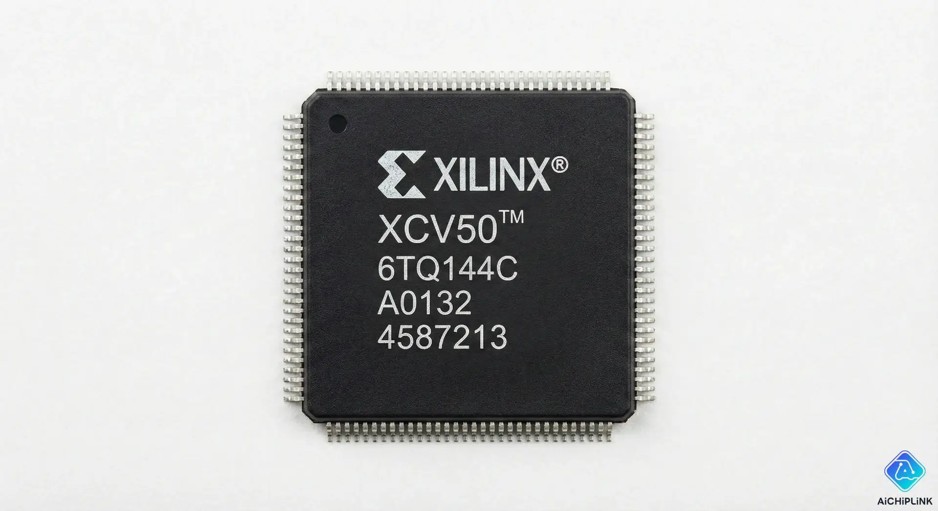
1.0 What is the XCV50-6TQ144C? (Datasheet Explained)
The XCV50-6TQ144C is a Field-Programmable Gate Array (FPGA) from the original Xilinx Virtex series. It is an SRAM-based device, meaning it is reconfigurable and volatile (it requires an external boot source like a PROM).
1.1 The Original Virtex Family: The 2.5V Pioneer
The Virtex family was revolutionary because it moved the industry from 5V logic to a high-performance **2.5V core architecture**. * **System Gates:** 57,906. * **Logic Cells:** 1,728. * **Feature Set:** It introduced Delay-Locked Loops (DLLs) for clock management and dedicated BlockRAM, features that are now standard in every modern FPGA.1.2 Decoding the Part Number: Speed Grade -6 & TQ144
The part number tells you exactly what this device is capable of:- XCV: Family (Xilinx Virtex).
- 50: Density (50,000 System Gates).
- -6: Speed Grade (Fastest).
- Note: The Virtex family typically came in -4, -5, and -6 grades. The -6 is the highest performance version, offering faster clock rates and shorter propagation delays than the standard -4.
- TQ: Package Type (Thin Quad Flat Pack).
- 144: Pin Count (144 pins).
- C: Temperature Grade (Commercial: 0°C to +85°C).
1.3 Obsolescence Status: A Vital MRO Component
> **Status: OBSOLETE / END-OF-LIFE (EOL)** > > The XCV50-6TQ144C is **obsolete**. Xilinx (now AMD) no longer manufactures it. > > **Implication:** This part is critical for repair. Because it uses a specific package (TQ144) and voltage (2.5V), you cannot simply swap it with a modern FPGA. You must source genuine legacy stock from specialized distributors like **AichipLink** to ensure compatibility.2.0 XCV50-6TQ144C Key Technical Specifications
If you are replacing a failed chip, these specs must match to ensure the system timing remains valid.
2.1 Core Logic, Block RAM, and DLLs
| Feature | Specification |
|---|---|
| System Gates | 57,906 |
| Logic Cells | 1,728 |
| CLB Array | 16 x 24 |
| Total Block RAM | 32,768 bits (32k) |
| Max User I/O | 98 (in TQ144 package) |
| Delay-Locked Loops (DLLs) | 4 |
| Speed Grade | -6 (High Performance) |
2.2 Operating Voltage: The 2.5V Core Constraint
The Virtex architecture requires strict power supply management. * **VCCINT (Core Voltage):** **2.5V** (±5%). This powers the internal logic and BlockRAM. * **VCCO (I/O Voltage):** **3.3V, 2.5V, or 1.5V**. The TQ144 package has separate banks that can be powered independently to interface with different logic standards (LVTTL, LVCMOS, etc.).Critical Warning: Unlike older XC4000 parts, this is not a 5V core device. Applying 5V to VCCINT will destroy it instantly.
3.0 Pinout and Package Details (TQ144)
The TQ144 is a surface-mount Thin Quad Flat Pack with leads on all four sides.
3.1 Understanding the 144-Pin TQFP Package
* **Leads:** Gull-wing leads on 0.5mm pitch. * **Mounting:** Surface Mount Technology (SMT). * **Advantages:** Unlike BGA packages, the TQFP leads are visible, making it much easier to inspect solder joints and probe pins for debugging during repairs.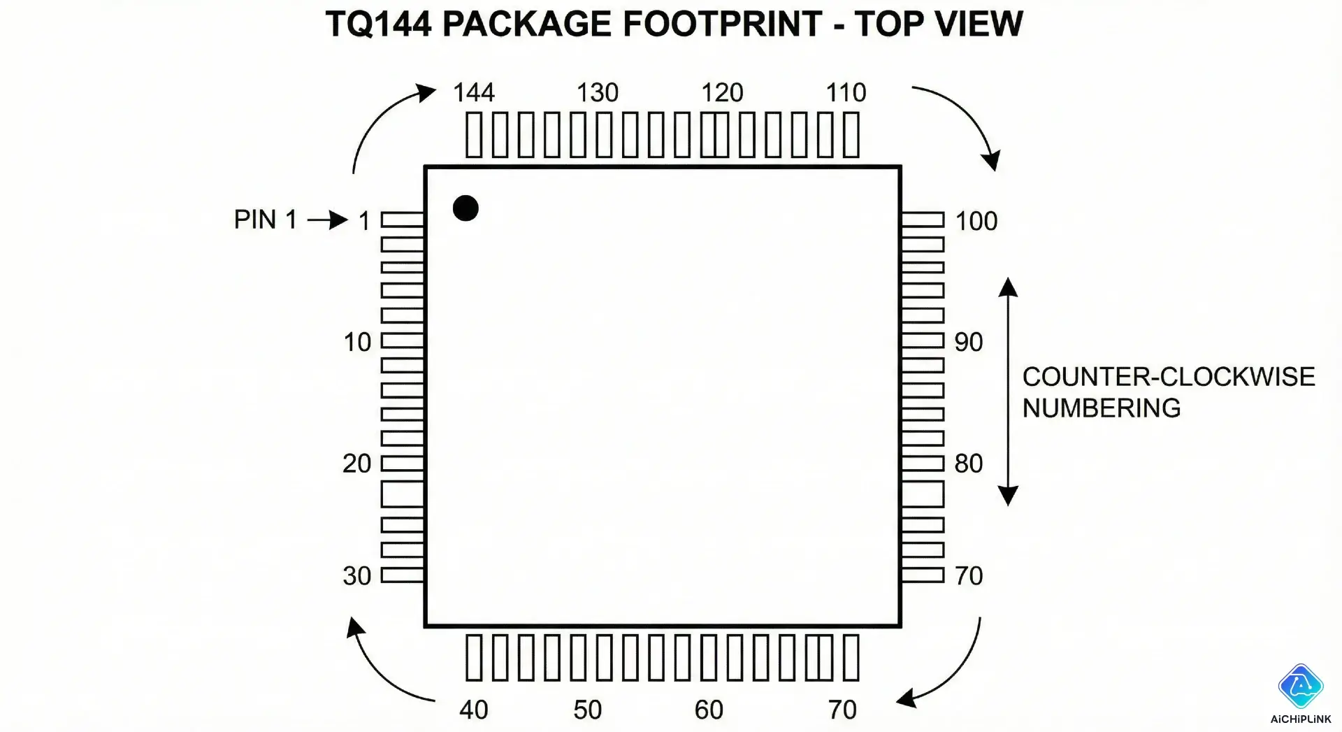
3.2 Key Pin Functions: VCCINT, VCCO, and Configuration
When troubleshooting a board, check these pins first: * **VCCINT Pins:** Must measure 2.5V. * **VCCO Pins:** Must measure the I/O voltage (usually 3.3V). * **PROGRAM_B:** Active Low configuration reset. If this is stuck low, the FPGA will never start. * **DONE:** This pin goes High when configuration is successful. **If the DONE pin is low, the FPGA is unconfigured or faulty.** * **TDI, TCK, TMS, TDO:** JTAG pins for testing and programming.4.0 Programming and Maintenance Guide
You've found a replacement chip. Now, how do you get the bitstream into it?
4.1 Required Software: Legacy Xilinx ISE 14.7
You **cannot** use the modern Vivado software for the Virtex XCV50. * **Required Software:** **Xilinx ISE Design Suite**. * **Version:** ISE 14.7 (Windows 10 version or VM version) is standard. Older versions like ISE 10.1 also work well. * **Cable:** A **Xilinx Platform Cable USB** (Model DLC9G or DLC10) is required for JTAG programming.4.2 Configuration: SelectMAP and Serial Modes
The XCV50 is volatile. It loads its configuration from an external source at power-up. * **Serial PROM:** Often paired with an **XC1700** (OTP) or **XC18V00** (Flash) configuration PROM. * **SelectMAP:** In some systems, a microcontroller writes the configuration data to the FPGA via an 8-bit parallel bus (SelectMAP mode). * **Troubleshooting:** If the FPGA fails to boot, check the configuration PROM first. These are often the point of failure in aged systems.4.3 Replacement Strategy for Legacy Systems
If you have a failed XCV50-6TQ144C: 1. **Match the Speed:** You need a **-6** or faster. Do **not** use a -4 or -5, as they may be too slow for the system's timing requirements. 2. **Match the Temp:** You can use an "I" (Industrial) grade to replace a "C" (Commercial) grade, but not vice-versa. 3. **Verify Authenticity:** Counterfeits are common. Ensure your supplier performs functionality testing or X-ray verification.In Conclusion
The XCV50-6TQ144C is a legend of the FPGA world. While it may be two decades old, its role in maintaining critical industrial infrastructure is as important as ever. Understanding its 2.5V architecture, the high-performance "-6" speed grade, and the TQ144 package is essential for any engineer tasked with keeping these legacy systems alive.
If you are facing a line-down situation and need this hard-to-find part, don't gamble on unverified sources. Explore our inventory of legacy FPGAs or contact AichipLink today to secure genuine, tested components for your repair needs.

Written by Jack Elliott from AIChipLink.
AIChipLink, one of the fastest-growing global independent electronic components distributors in the world, offers millions of products from thousands of manufacturers, and many of our in-stock parts is available to ship same day.
We mainly source and distribute integrated circuit (IC) products of brands such as Broadcom, Microchip, Texas Instruments, Infineon, NXP, Analog Devices, Qualcomm, Intel, etc., which are widely used in communication & network, telecom, industrial control, new energy and automotive electronics.
Empowered by AI, Linked to the Future. Get started on AIChipLink.com and submit your RFQ online today!
Frequently Asked Questions
Is the XCV50-6TQ144C obsolete?
Yes, the XCV50-6TQ144C and the entire original Virtex family are obsolete (End-of-Life). They are no longer manufactured by Xilinx (AMD) and are available only through the surplus and legacy component market.
Can I replace an XCV50-4TQ144C with an XCV50-6TQ144C?
Yes. The **-6** is a faster speed grade than the **-4**. A faster FPGA can almost always replace a slower one because it meets or exceeds all timing requirements. This makes the -6 a versatile replacement part.
What voltage does the XCV50 require?
The XCV50 requires a **2.5V** supply for its internal core (VCCINT). The I/O banks (VCCO) can be powered by 3.3V, 2.5V, or other voltages depending on the I/O standard used.
Can I replace the TQ144 package with a BG256?
No. The **TQ144** (Quad Flat Pack) and **BG256** (Ball Grid Array) are completely different physical packages with different pinouts. They are not interchangeable without redesigning the circuit board.
Is the XCV50-6TQ144C 5V tolerant?
The Virtex inputs can be **5V tolerant** <em>if</em> configured correctly with external resistors and specific I/O standards, but natively, it is a 3.3V/2.5V device. Connecting 5V directly to VCC pins will destroy it.